Core Principles and Operation
Modular Research Platform
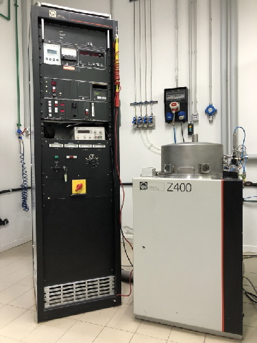
The Z400 is an advanced Physical Vapor Deposition (PVD) system, evolved from diode technology to Magnetron Sputtering (MS). Designed for high efficiency, it uses magnetic fields to confine the plasma. As a laboratory system, the Leybold-Heraeus LH Z400 MS system makes it possible to develop film and coat compact components. The system is equipped with a vacuum chambers and an R.F. (Radio Frequency) network and allows 3 targets to be installed simultaneously. With the variety of available target materials and the possibility of using a number of different reactive gases, the LH Z400 supplies film systems for a number of diverse applications.
Versatility and Power
- Extreme Thermal Control: Heating up to 550°C for crystallinity control.
- Material Versatility: Can deposit almost any solid material, including metals, alloys, semiconductors, and insulators/ceramics, handling even high melting point materials.
- High Adhesion: The high kinetic energy of the sputtered atoms ensures excellent adhesion between the deposited film and the substrate (silicon wafer).
- Uniformity and Purity: Allows precise control over film thickness and uniformity across large areas, essential for high-density integrated circuit mass production.
Application Sectors
- Electronics: Semiconductors and Transparent Conductive Oxides (TCO).
- Tribology: Ultra-hard DLC (Diamond-Like Carbon), Nitride, Carbide films.
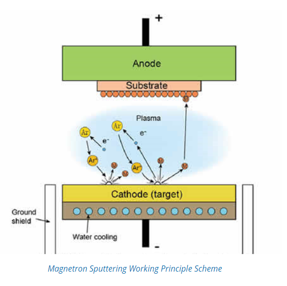
Operating Principle
Magnetron sputtering is a physical vapor deposition technique, which allows a good film adhesion to the substrate, and a high control on the thickness, uniformity and composition of the deposited material. By first creating a gaseous plasma and then accelerating the ions from this plasma into some source material (a.k.a. “target”), the source material is eroded by the arriving ions via energy transfer and is ejected in the form of neutral particles – either individual atoms, clusters of atoms or molecules. As these neutral particles are ejected, they will travel in a straight line unless they come into contact with something – other particles or a nearby surface. If a “substrate” such as a Si wafer is placed in the path of these ejected particles, it will be coated by a thin film of the source material. In order to create the plasma, atoms of an inert gas (frequently Ar) are introduced into the HV (High Vacuum) chamber and a negative bias voltage is applied to the target. Free electron are immediately accelerated by the electron field in proximity to the target and ionize by collision the Ar atoms leaving Ar+ ions. This cascade process ignites the plasma. At this point, positively charged Ar+ ions are accelerated towards the negatively biased electrode, striking the surface and releasing source material and more free electrons by energy transfer. In magnetron sputtering, permanent magnets are located behind the target in order to confine the free electrons in a magnetic field directly above the target surface. This provides a double advantage: first, the free electrons, which are rejected by the negatively charged target, are prevented from bombarding the substrate, which would cause overheating and structural damage; second, the circuitous path carved by the free electrons along the lines of the magnetic field enhances the probability of ionizing neutral Ar atoms by several orders of magnitude. This increase in available ions significantly increases the rate at which target material is eroded and subsequently deposited onto the substra